-
Give us a call +86 -755-25432352
-
Email us info@urbanmines.com
-
Come & visit us No. 11, Bld. C, Hengmingzhu Tech. Industrial Park, Shajing Subdistrict, Bao'an District, Shenzhen, Guangdong, China
Give us a call +86 -755-25432352
Email us info@urbanmines.com
Come & visit us No. 11, Bld. C, Hengmingzhu Tech. Industrial Park, Shajing Subdistrict, Bao'an District, Shenzhen, Guangdong, China
Unlocking the Semiconductor Silicon Revolution: China's Strength in High-Purity 6N Crystal Boron Dopants
At the pinnacle of precision manufacturing, every performance leap in semiconductor silicon begins with precise control at the atomic level. The key to achieving this control lies in ultra-high-purity crystalline boron dopants. As an indispensable foundational material for the global cutting-edge electronics industry, 6N crystalline boron (purity ≥99.9999%), with its irreplaceable properties, has become the "invisible architect" shaping modern chips and power devices.
Why is 6N crystalline boron the "lifeline" of semiconductor silicon?
Precise P-type "Switch": When 6N boron atoms are precisely introduced into the semiconductor silicon lattice, they create crucial "holes" that give the silicon wafer its P-type conductivity. This is the foundation for building diodes, field-effect transistors (FETs), and even complex integrated circuits.
The cornerstone of performance: The efficiency, stability, and switching speed of semiconductor devices are critically dependent on the uniformity and purity of doping. Any trace impurities (such as carbon, oxygen, and metallic elements) can act as carrier traps, leading to increased leakage current and device failure. 6N boron crystalline controls impurity levels to the parts-per-billion (ppb) level, ensuring the ultimate purity and reliability of semiconductor silicon electrical performance.
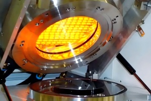
A guardian of high-temperature processes: With a melting point above 2300°C, crystalline boron possesses exceptional thermal stability. During demanding processes such as silicon single crystal growth (Czochralski method) or high-temperature diffusion/ion implantation annealing, 6N crystalline boron maintains structural stability without introducing unexpected volatiles or decomposition products, ensuring process controllability and repeatability.
Proven in cutting-edge global applications: A trusted choice for Korean and Japanese customers
Case 1 (South Korean semiconductor silicon wafer manufacturer): UrbanMines ' 6N boron powder (99.9999% purity, 2-3mm particle size) was used as a key dopant in a Czochralski single crystal furnace to grow high-quality P-type semiconductor silicon ingots with a specific resistivity range for the manufacture of advanced logic chips.
Case 2 (Japanese silicon epitaxial wafer/device manufacturer): UrbanMines was designated to purchase 6N pure boron dopant (purity 99.9999%, particle size -4+40 mesh). This dopant is used in epitaxial growth or high-temperature diffusion processes to precisely control the boron concentration distribution in the semiconductor silicon epitaxial layer or junction region, meeting the stringent requirements of high-voltage power devices (such as IGBTs).
--
China Supply: Strategic Advantages of 6N Crystalline Boron
Facing the growing high-end demand from global semiconductor core regions such as South Korea, Japan, and the United States, our company has established significant production and supply advantages in the field of high-purity boron materials:
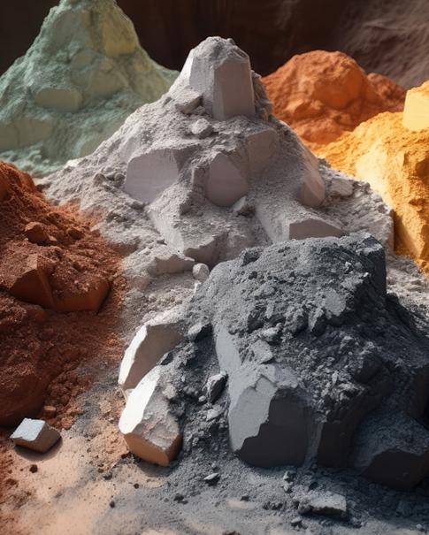
1. Technological breakthroughs and economies of scale: Through continuous research and development, our company has mastered the large-scale production process for high-purity β-rhombohedral boron (the most stable form). This allows us to offer a full range of purity levels, from 99% to 6N (99.9999%) and even higher. Our stable production capacity allows us to meet large orders from major global customers (as demonstrated by our monthly demand for 50kg of amorphous boron for solar applications).
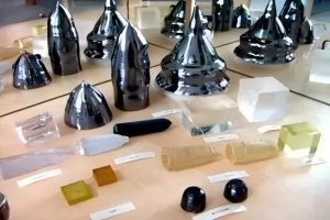
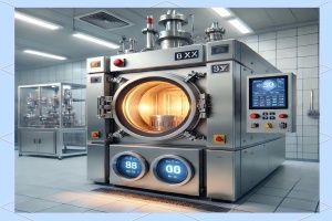
2. Strict quality control system: Benchmarked against international semiconductor-grade standards, we have established an ultra-clean management and control system for the entire process, covering raw material screening, reaction synthesis, purification and refining (such as regional melting and vacuum distillation), crushing and grading, and packaging. This ensures that each batch of 6N boron crystals has excellent traceable consistency.
3. Deep Customization Capabilities: Our company deeply understands the precise requirements of semiconductor processes for boron form (granules, powders) and particle size (e.g., D50 ≤ 10μm, -200 mesh, 1-10mm, 2-4μm, etc.). As stated in the document, "custom production is also possible if specific particle size requirements are met." This flexible responsiveness is key to winning high-end customers in South Korea, Japan, and other countries.
4. Industrial Chain Collaboration and Cost Advantages: Leveraging a comprehensive domestic industrial system and raw material resources, our 6N crystalline boron not only ensures top-tier quality but also boasts superior supply chain resilience and comprehensive cost competitiveness, providing stable, reliable, and cost-effective key material support for the global semiconductor manufacturing industry.
Conclusion: China's boron materials take the lead in empowering future chips
From the core processors of smartphones to the power chips that power the "brains" of new energy vehicles, the performance boundaries of semiconductor silicon continue to be defined by the purity and precision of 6N crystalline boron dopants. China's high-purity boron industry, with its solid technological expertise, strict quality control, flexible customization capabilities, and robust production capacity, is becoming a key driver of global semiconductor innovation.
Choosing a reliable Chinese 6N boron crystal supplier means choosing a clear path to the future of semiconductor silicon. Deeply engaged in the field of high-purity boron, we possess the production capabilities and customized solutions to meet the most demanding semiconductor applications. Contact us today to inject powerful and precise Chinese boron power into your cutting-edge semiconductor silicon devices!


Copyright @ 2010-2026 UrbanMines Tech. Co., Ltd. All Rights Reserved.
 IPv6 Network Supported