
Cheap PriceList for Dysprosia (CAS No. 1308-87-8) - Purchasing & Recycling IC Wafers – UrbanMines
Cheap PriceList for Dysprosia (CAS No. 1308-87-8) - Purchasing & Recycling IC Wafers – UrbanMines Detail:
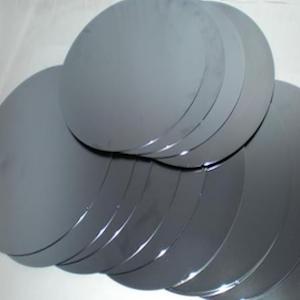
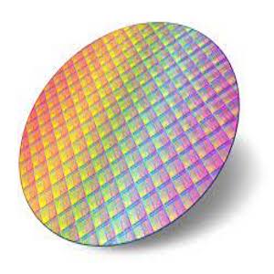
Prime grade Silicon Wafers are the best and the highest grade of silicon wafers.It can be used for device manufacturing, with properties usually including extremely smooth surface and low Total Thickness Variation (TTV).Its excellent quality and polished surface with the ability to offer tighter resistivity specs are something that makes Prime grade wafers the best.It offers exceptional quality, polished surface and have an extended lifespan.
| 6 inch(150mm),8 inch(200mm),12 inch(300mm) | 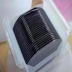 |
 |
Test Grade Wafer/Dummy Wafer
Dummy wafer (also called as test wafers) is a Si dummy wafer mainly used for experiment and test.Test grade wafers are high quality but have less stringent properties than prime grade wafers. Accordingly, reclaimed wafers are mostly applied as dummy grade wafers (test wafers). Test grade wafers are often used in applications that require a large quantity of wafers for equipment and fabrication testing. In each process, film thickness, pressure resistance, reflection index and presence of pinball are measured using dummy wafers (test wafers).
| 6 inch(150mm),8 inch(200mm),12 inch(300mm)
|
 |
 |
Test Grade Wafer/Monitor Wafers
Monitor wafers are the bare silicon wafers to be used in the case that an adjustment is required in each production step prior to the actual IC production.For example, when the conditions of each process are set, such as the case of measuring tolerance of device against ( the variation of ) substrate thickness, coinroll silicon wafers for spacer wafers are being used as a substitution of high-standard and high value wafers. Moreover, they are also used for the monitoring purpose in the process together with product wafers.
| 6 inch(150mm),8 inch(200mm),12 inch(300mm) | 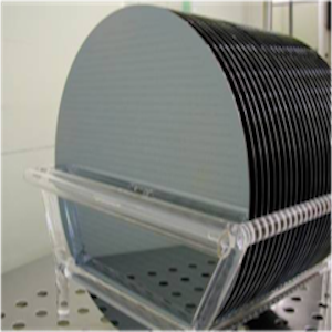 |
 |
Reclaimed Wafer
Due to the high costs of prime grade silicon and large volumes consumed,many semiconductor facilities use reclaimed wafers to optimize and monitor their manufacturing processes and equipment. Reclaim involves removing unwanted material from the wafer with a combination of dry and wet processes, and then polishing & cleaning the wafer to restore the silicon surface to a usable grade. The nature of the typical process requires some removal of silicon. The source of the reclaimed wafers comes from the monitor wafers and the dummy wafers but not the defect wafers in the semiconductor fab. The reclamation of these monitor wafers and dummy wafer to refurbish can dramatically lower the running cost of a factory.
| 6 inch(150mm),8 inch(200mm),12 inch(300mm)
|
 |
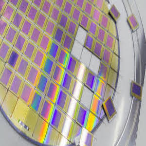 |
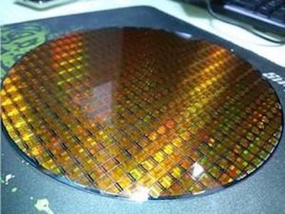
Sputtered Wafer
The sputter process has been designed to deposit ultra-clean metal and dielectric films.All wafer processing, including metal deposition, is performed inside cleanroom. An in-situ RF etch is necessary to the process to ensure good film adhesion and ohmic contact to underlying conductive layers. All sputter films are available on silicon wafers sizes up to 300mm in diameter. We have the demand of wide variety of sputtered non-precious metals, dielectric films, and silicon. The Most Popular Sputtered Films Include: Copper, Aluminum, Nickel and others.
| 150〜300mm | 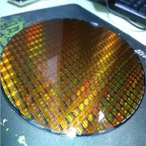 |
 |
Other Semiconductor Wafer
Patterned Wafer. Patterned silicon wafers have the same quality and cleanliness requirements as standard patterned silicon wafer appearance. (Unpatterned)Bare Wafer.A large bare silicon wafer, or SDB, is a silicon wafer that is over eight inches in diameter. Efficient semiconductor production and manufacturing processes start with quality control of bare silicon and epitaxial wafers. Metal Septum Wafer. Non-Metal Septum Wafer. Others semiconductor wafer.
| 200&300mm | 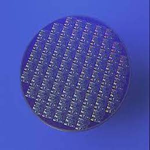 |
 |
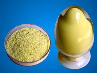
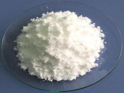
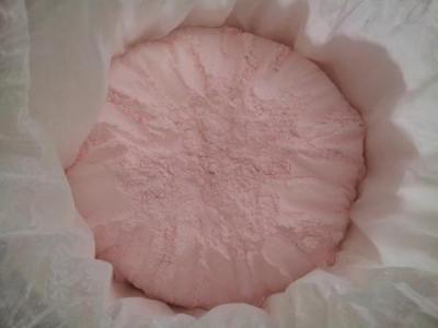
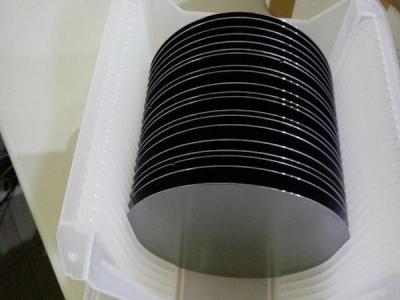
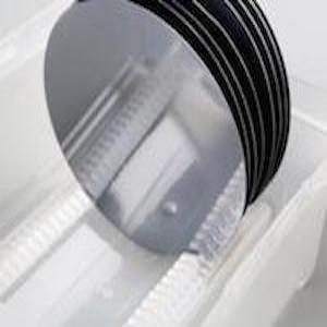
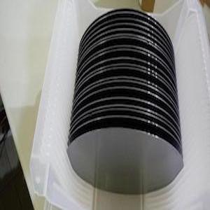
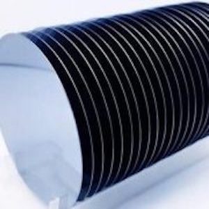
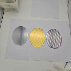
Product detail pictures:


Related Product Guide:
We stick to our enterprise spirit of Quality, Efficiency, Innovation and Integrity. We aim to create more value for our customers with our rich resources, advanced machinery, experienced workers and excellent services for Cheap PriceList for Dysprosia (CAS No. 1308-87-8) - Purchasing & Recycling IC Wafers – UrbanMines , The product will supply to all over the world, such as: Comoros, Spain, Holland, Company name, is always regarding quality as company' s foundation, seeking for development via high degree of credibility , abiding by ISO quality management standard strictly, creating good -ranking company by spirit of progress-marking honesty and optimism.
The company has a good reputation in this industry, and finally it tured out that choose them is a good choice.